| . |  |
. |
Washington DC (SPX) Apr 29, 2011 Researchers at the National Institute of Standards and Technology (NIST) have shown that the electronic properties of two layers of graphene vary on the nanometer scale. The surprising new results reveal that not only does the difference in the strength of the electric charges between the two layers vary across the layers, but they also actually reverse in sign to create randomly distributed puddles of alternating positive and negative charges. Reported in Nature Physics,* the new measurements bring graphene a step closer to being used in practical electronic devices. Graphene, a single layer of carbon atoms, is prized for its remarkable properties, not the least of which is the way it conducts electrons at high speed. However, the lack of what physicists call a band gap-an energetic threshold that makes it possible to turn a transistor on and off-makes graphene ill-suited for digital electronic applications. Researchers have known that bilayer graphene, consisting of two stacked graphene layers, acts more like a semiconductor when immersed in an electric field. According to NIST researcher Nikolai Zhitenev, the band gap may also form on its own due to variations in the sheets' electrical potential caused by interactions among the graphene electrons or with the substrate (usually a nonconducting, or insulating material) that the graphene is placed upon. NIST fellow Joseph Stroscio says that their measurements indicate that interactions with the disordered insulating substrate material causes pools of electrons and electron holes (basically, the absence of electrons) to form in the graphene layers. Both electron and hole "pools" are deeper on the bottom layer because it is closer to the substrate. This difference in "pool" depths, or charge density, between the layers creates the random pattern of alternating charges and the spatially varying band gap. Manipulating the purity of the substrate could give researchers a way to finely control graphene's band gap and may eventually lead to the fabrication of graphene-based transistors that can be turned on and off like a semiconductor. Still, as shown in the group's previous work**, while these substrate interactions open the door to graphene's use as a practical electronic material, they lower the window on speed. Electrons do not move as well through substrate-mounted bilayer graphene; however, this may likely be compensated for by engineering the graphene/substrate interactions. Stroscio's team plans to explore further the role that substrates may play in the creation and control of band gaps in graphene by using different substrate materials. If the substrate interactions can be reduced far enough, says Stroscio, the exotic quantum properties of bilayer graphene may be harnessed to create a new quantum field effect transistor.
Share This Article With Planet Earth
Related Links National Institute of Standards and Technology (NIST) Carbon Worlds - where graphite, diamond, amorphous, fullerenes meet
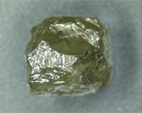 Diamonds shine in quantum networks
Calgary, Canada (SPX) Apr 27, 2011 When it comes to dreaming about diamonds, energy efficiency and powerful information processing aren't normally the thoughts that spring to mind. Unless, of course, you are a quantum physicist looking to create the most secure and powerful networks around. Researchers at the University of Calgary and Hewlett Packard Labs in Palo Alto, California, have come up with a way to use impurities i ... read more |
|
| The content herein, unless otherwise known to be public domain, are Copyright 1995-2010 - SpaceDaily. AFP and UPI Wire Stories are copyright Agence France-Presse and United Press International. ESA Portal Reports are copyright European Space Agency. All NASA sourced material is public domain. Additional copyrights may apply in whole or part to other bona fide parties. Advertising does not imply endorsement,agreement or approval of any opinions, statements or information provided by SpaceDaily on any Web page published or hosted by SpaceDaily. Privacy Statement |


 del.icio.us
 Digg
Digg Reddit
 YahooMyWeb
 Google