| . |  |
. |
|
|
. |
by Staff Writers Philadelphia PA (SPX) Jul 26, 2011
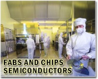
Renaissance architects demonstrated their understanding of geometry and physics when they built whispering galleries into their cathedrals. These circular chambers were designed to amplify and direct sound waves so that, when standing in the right spot, a whisper could be heard from across the room. Now, scientists at the University of Pennsylvania have applied the same principle on the nanoscale to drastically reduce emission lifetime, a key property of semiconductors, which can lead to the development of new ultrafast photonic devices. "When you excite a semiconductor, then it takes a few nanoseconds to get back to the ground state accompanied by emission of light," Agarwal said. "That's the emission lifetime. It's roughly the amount of time the light is on, and hence is the amount of time it takes for it to be ready to be turned on again. "If you're making a modulator, something that switches back and forth, you're limited by this time constant. What we've done is reduced it to less than a picosecond. It's more than a thousand times faster than anything currently available." In semiconductors, the excited state is when energy is present in the system, and the ground state is when there is none. Normally, the semiconductor must first "cool down" in the excited state, releasing energy as heat, before "jumping" back to the ground state, releasing the remaining energy as light. The Penn team's semiconductor nanowires, however, can jump directly from a high-energy excited state to the ground, all but eliminating the cool-down period. The advancement in emission lifetime is due to the unique construction of the team's nanowires. At their core, they are cadmium sulfide, a common nanowire material. But they are also wrapped in a buffer layer of silicon dioxide, and, critically, an outer layer of silver. The silver coating supports what are known as surface plasmons, unique waves that are a combination of oscillating metal electrons and of light. These surface plasmons are highly confined to the surface the silicon dioxide and silver layers meet. "The previous state of the art was taking a nanowire, just like ours, and laying it on a metal surface," Agarwal said. "We curved the metal surface around the wire, making a complete nanoscale plasmonic cavity and the whispering gallery effect." For certain nanowire sizes, the silver coating creates pockets of resonance and hence highly confined electromagnetic fields within the nanostructure. Emission lifetime can then be engineered by precisely controlling high intensity electromagnetic fields inside the light-emitting medium, which is the cadmium sulfide core. To reach an emission lifetime measured in femtoseconds, the researchers needed to optimally balance this high-confinement electromagnetic field with an appropriate "quality factor," the measurement of how good a cavity is at storing energy. To complicate matters, quality factor and confinement have an inverse relationship; the higher the quality-factor a cavity has the bigger it is and the smaller its confinement. However, by opting for a reasonable quality factor, the researchers could vastly increase the confinement of the electric field inside the nanowire by using resonant surface plasmons and get the record-breaking emission lifetime. This many-orders-of-magnitude improvement could find a home in a variety of applications such as LEDs, detectors and other nanophotonic devices with novel properties. "Plasmonic computers could make good use of these nanowires," Cho said. "We could increase modulation speed into the terahertz range whereas electronic computers are limited to a few gigahertz range." "The same physics governs emission and absorption, so these nanowires could also be used for increasing efficiency of absorption in solar cells," Agarwal said. The research was conducted by associate professor Ritesh Agarwal, postdoctoral fellows Chang-Hee Cho and Sung-Wook Nam and graduate student Carlos O. Aspetti, all of the Department of Materials Science and Engineering in Penn's School of Engineering and Applied Science. Michael E. Turk and James M. Kikkawa of the Department of Physics and Astronomy in the School of Arts and Sciences also contributed to the study. Their research was published in the journal Nature Materials.
|
. |
|
| The content herein, unless otherwise known to be public domain, are Copyright 1995-2011 - Space Media Network. AFP and UPI Wire Stories are copyright Agence France-Presse and United Press International. ESA Portal Reports are copyright European Space Agency. All NASA sourced material is public domain. Additional copyrights may apply in whole or part to other bona fide parties. Advertising does not imply endorsement,agreement or approval of any opinions, statements or information provided by Space Media Network on any Web page published or hosted by Space Media Network. Privacy Statement |

 del.icio.us
 Digg
Digg Reddit
 Google